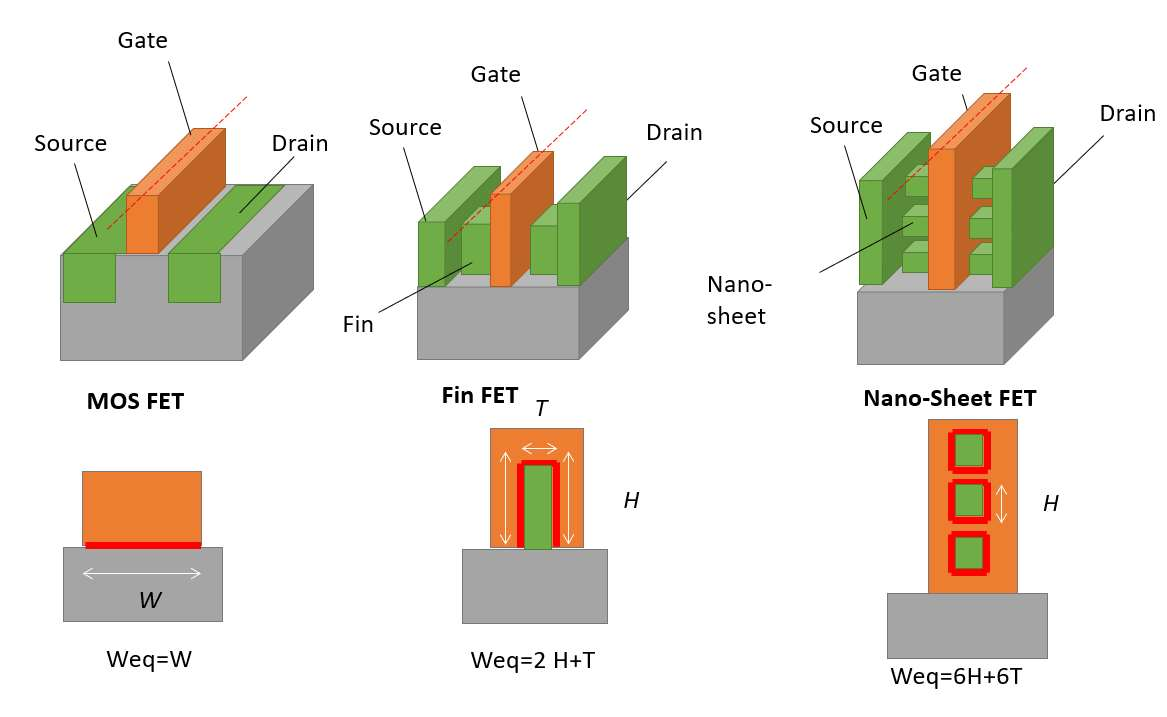
The adoption of nano-sheet FET should follow the adoption of FinFET with a 10-years shift. Is it anticipated that the 3-nm node will enable further gains in current drive while reducing the device surface, thus enabling smaller, faster and more energy-efficient chips. The three different categories of applications should remain: high performance computing (severs, data centers), general purpose (laptops, gaming), and low power (mobile, IoT) with significant differences in terms of acceptable leakage current (IOFF).
No n-well layer is required anymore as the device channel is totally surrounded by the gate, without any influence of the substrate as for MosFET & FinFET. Therefore, no polarization is required too, which enables to place n & p devices much closer to each other than previous technologies.